
PCBs are most commonly made out of fiberglass, composite, epoxy, or another composite material. Most PCBs for simple electronics are simple and composed of only a single layer. More sophisticated hardware such as computer graphics cards or motherboards can have multiple layers, sometimes up to twelve.
Anatomy of a Printed Circuit Board (PCB)
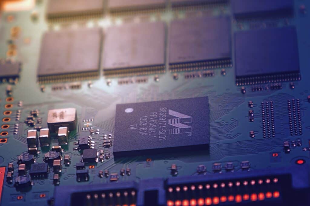
As we all know what circuit boards look like: They’re thin, rigid, and usually rectangular, with components attached to one or both surfaces. The top and bottom are generally colored in dark blue or green. Lines running between the components have a slightly different color. In addition to the top and bottom sides, modern circuit boards have internal planes called layers. Internal layers don’t have components but may contain metal lines the carry electricity to and from the components on the top and bottom. For example, the circuit board in the iPhone handset has 10 layers.
Layers are critically important in PCB design, so circuit board are commonly divided into three categories: single-sided, double-sided, or multilayer. This section discusses each of these categories and the manner in which the circuit boards are constructed.
Single-sided boards
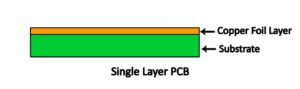
The body of a single-sided board is made of a hard, nonconductive material, typically fiberglass epoxy-resin, or FR4. Some literature refers to a board’s material as substrate, the substrate thickness is given in thousandths of inches called mils (1 mil = 0.001 in). standard board thicknesses are 31 mils, 39 mils and 62 mils. A thin layer of metal is attached (usually glued or electrodeposited) to one side of the board, and will call this the top side. This metal is almost always copper, which is inexpensive and provides a low-resistance path for electricity.
Double-side boards
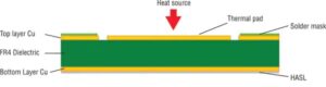
As the number of components on a board increases, so do the number of traces. In many instances, the full set of traces can’t be connected on a single plane without intersecting one another. To solve this problem, traces need a way to jump over other traces. This jumping is made possible by adding copper to the board’s bottom side. This bottom side may also support additional components. A board with copper on both sides is called a double-sided board.
Multilayer Boards
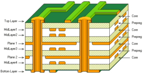
Double-sided boards enable more complex routing than single-sided boards, but sometimes two layers still aren’t enough. This occurs frequently when designing circuit whose components have hundreds of closely spaced leads. It’s also important for designs that require entire layers for ground or power supply. To resolve these issues, board designers create multilayer board designs. In essence, a multilayer board is a group of double-sided board sandwiched together using a material called prepreg. Similar to glue, prepreg is soft to begin with but hardens when heat and pressure are applied. A board’s arrangement of core and prepreg layers in a multilayer board is called its stack-up.