PCB Fabrication and Assembly
Printed circuit board fabrication can be defined as a process of putting together the layers of the board along with particular surface patterns before making it fully usable for electronics manufacturing. In a way, it is an assembly method that can be done either by the manufacturing firms themselves or by outsourcing the service to third parties specializing in PCB fabrication.
The process of printed circuit board fabrication starts with a design or a diagram using client provided specifications and requirements. The Printed circuit board layout is an important part of the fabrication process. It involves a schematic design, which is created by the specialists after considering factors like: what the Printed circuit board is required to do, its functional attributes, and under what conditions would it be used. These details are provided by the customers or the clients to the PCB manufacturers who use the information for successful PCB fabrication.
What is the PCB fabrication process?
PCB fabrication is the process or procedure that transforms a circuit board design into a physical structure based upon the specifications provided in the design package. This physical manifestation is achieved through the following actions or techniques: Imaging desired layout on copper clad laminates. There have a few other terms and their interrelationships as below: –
- PCB Development – can be defined as the process of taking a circuit board design from the design to the production. This typically includes three stages – design, manufacturing and testing. And for all but the simplest designs, this process is iterative with the objective of arriving at the highest quality design within the development time allotted.
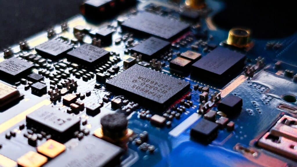
- PCB Manufacturing – can be defined as the construction o your board design. This is a two-step process that begins with board fabrication and ends with printed circuit board assembly (PCBA).
- PCB Testing – sometimes referred to as bring up. is the third stage of PCB development; performed after manufacturing. Testing during development is done to evaluate the board’s ability to perform its intended operational functionality. During this stage, any error or areas where the design should be modified to improve performance are identified and another cycle is initiated to incorporate the design changes.
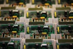
- PCB Assembly – PCBA is the second step or stage of PCB manufacturing in which the board components are mounted to the bare board through a soldering process.