
Optimized PCB Design for Functionality, Reliability, and Manufacturability
A Good PCB Design
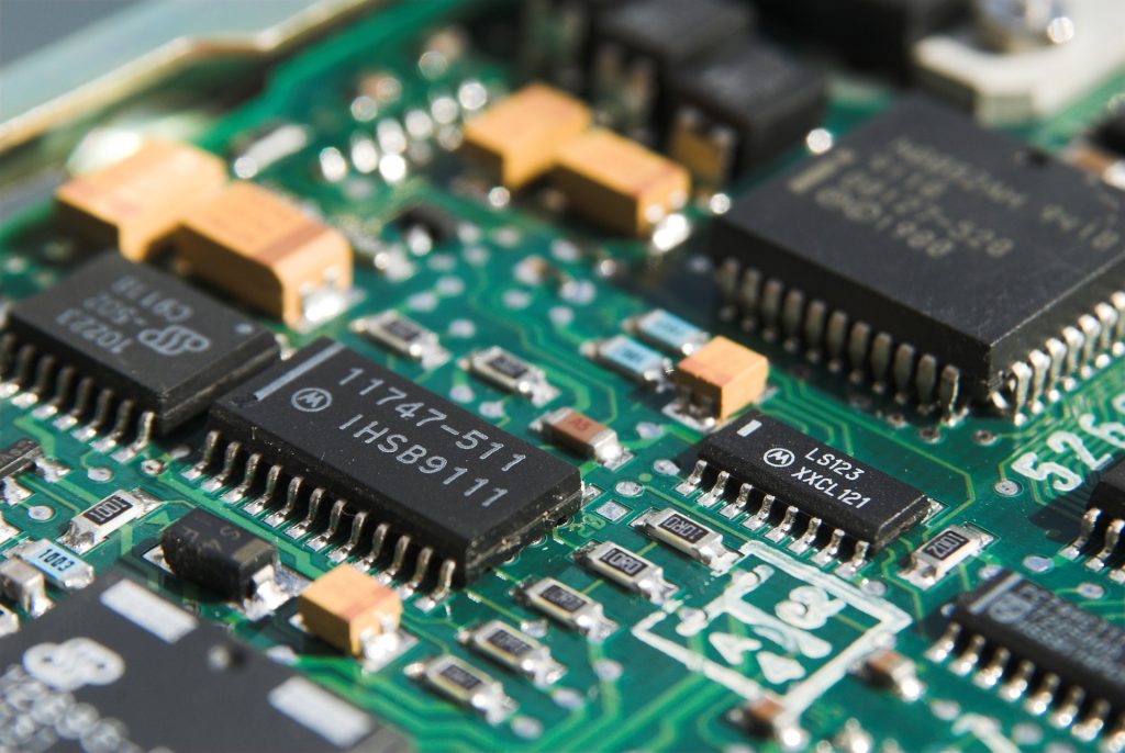
A good PCB (Printed Circuit Board) design is one that is optimized for functionality, reliability, and manufacturability. Here are some key factors to consider when designing a good PCB:
Functionality: To ensure that the PCB meets the functional requirements, it is important to carefully select and place components, and route the traces in a way that minimizes interference between signals. This involves paying close attention to the electrical characteristics of the circuit, such as the signal frequency, voltage levels, and impedance matching. Simulation tools such as SPICE (Simulation Program with Integrated Circuit Emphasis) can be used to verify the circuit performance before the design is finalized.
Reliability: A reliable PCB design considers factors such as thermal management, EMI/EMC, and mechanical stresses that the board may be subjected to. Thermal management involves proper placement of components, heat sinks, and vias to dissipate heat generated by the components. EMI/EMC involves the careful routing of signals to minimize electromagnetic interference and ensure the PCB complies with relevant regulations. Mechanical stresses may include shock and vibration, which can be mitigated through the use of proper mounting techniques, support structures, and material selection.
Manufacturability: A PCB design that is optimized for manufacturability considers factors such as the use of standard components, design for ease of assembly, and minimizing the number of layers and vias. It is important to ensure that the design is compatible with the chosen manufacturing process, whether it is through-hole, surface-mount, or a combination of both. To minimize errors during manufacturing, it is important to follow industry best practices such as keeping traces and components within the recommended spacing and clearance guidelines.
Design for Testability (DFT): DFT is an important consideration in PCB design to ensure that the board can be tested accurately and efficiently. This involves adding test points, designing the circuit in a way that allows for easy access to components and signals, and using test software to automate testing. By designing the PCB for testability, defects can be detected early in the manufacturing process and fixed before the board is shipped.
Documentation: Clear and concise documentation is essential for a good PCB design. This includes detailed schematics, board layout files, and a complete BOM. The documentation should be organized and easy to navigate, with all necessary information included such as component specifications, reference designators, and manufacturing notes. By providing thorough documentation, the PCB can be manufactured and assembled accurately and efficiently.
By considering these factors and working closely with a manufacturer, a good PCB design can be achieved that is optimized for functionality, reliability, and manufacturability.
7 Steps to Improve Your PCB Design Skills
Introduction:
PCB design is an essential aspect of modern electronics. It involves designing and laying out printed circuit boards that serve as the foundation for electronic devices. Whether you are a beginner or an experienced PCB designer, there is always room for improvement. In this blog, we will explore 7 steps that you can take to improve your PCB design skills.
Step 1: Start with the basics of electronics
Before you start designing PCBs, it’s important to have a solid foundation in electronics. This includes understanding electronic components and circuits, as well as circuit analysis techniques. You can start by learning the basics of DC and AC circuits, Ohm’s law, Kirchhoff’s laws, and basic electronic components such as resistors, capacitors, inductors, and diodes.
Step 2: Choose the right design software
There are many PCB design software options available, and it’s important to choose the one that best suits your needs. Some popular options include Altium Designer, Eagle PCB, KiCad, OrCAD, and PADS. Look for software that has a user-friendly interface, good customer support, and a wide range of features to help you design your PCB effectively.
Step 3: Learn the design rules
PCB design is subject to certain design rules that must be followed to ensure that the circuit works correctly and reliably. These rules include trace width, spacing, and clearance, as well as component placement and orientation. The design rules also cover aspects such as signal integrity, thermal management, and EMI/EMC compliance. It’s essential to learn and follow these design rules to produce a functional PCB.
Step 4: Use libraries
Most PCB design software includes libraries of pre-built components that can be easily placed on the board. Using libraries can save you time and ensure that your design is accurate. You can also create your own custom libraries for components that are not included in the software.
Step 5: Pay attention to placement and routing
The placement of components and routing of traces on the PCB is critical to the performance of the circuit. You should place components in a logical and organized way, paying attention to factors such as signal flow, power delivery, and heat dissipation. Routing the traces correctly is equally important, as it can affect signal integrity and EMI/EMC compliance. Be sure to use the design rules to guide your placement and routing decisions.
Step 6: Consider manufacturability
When designing a PCB, you should keep manufacturability in mind. This means designing the PCB so that it can be easily manufactured using standard processes and materials. Consider factors such as board size, component density, and assembly processes when designing your PCB. Also, make sure to generate the necessary manufacturing files such as Gerber files, drill files, and bill of materials (BOM) so that your PCB can be manufactured with ease.
Step 7: Keep learning
PCB design is a dynamic field that is constantly evolving. Keep up with the latest technologies and techniques by reading industry publications, attending conferences and workshops, and taking online courses. Learning new skills and techniques will help you become a better PCB designer and keep you competitive in the job market.
Conclusion:
By following these 7 steps, you can improve your PCB design skills and produce high-quality PCBs that meet the design requirements. Remember to start with the basics of electronics, choose the right design software, learn the design rules, use libraries, pay attention to placement and routing, consider manufacturability, and keep learning. With practice and dedication, you can become a skilled PCB designer who can create complex circuits and systems with ease
Optimized PCB Design for Functionality, Reliability, and Manufacturability Read More »