Printed Circuit Board Assembly

Revolutionizing Electronic Design and Manufacturing: The Power of AI Technology

In recent years, the integration of Artificial Intelligence (AI) technology into various industries has revolutionized processes and improved efficiency. The electronic design and manufacturing sector is no exception. With its ability to analyze vast amounts of data, learn patterns, and make intelligent decisions, AI has become a game-changer in optimizing electronic design, enhancing manufacturing processes, and driving innovation. In this article, we will explore in detail the significant impact of AI technology on electronic design and manufacturing.

Design Optimization:

AI technology has transformed the electronic design process by enabling advanced optimization techniques. Designers can leverage AI algorithms to explore a vast design space, quickly evaluate numerous possibilities, and identify the most efficient and effective designs. AI algorithms can analyze design constraints, performance objectives, and historical data to generate optimized circuit layouts, improve power efficiency, reduce electromagnetic interference, and enhance overall design performance.

For example, AI-based optimization algorithms can analyze a wide range of circuit parameters and constraints to find the optimal trade-off between power consumption, performance, and cost. These algorithms can identify design solutions that human designers might overlook, leading to more efficient and innovative electronic designs.

Predictive Maintenance:

In the manufacturing phase, AI technology plays a crucial role in predictive maintenance. By continuously monitoring sensors and data points, AI algorithms can detect anomalies, predict equipment failures, and recommend preventive actions. This proactive approach minimizes unplanned downtime, reduces maintenance costs, and optimizes production efficiency.

AI-powered predictive maintenance algorithms can analyze real-time data, historical records, and equipment performance patterns to accurately forecast maintenance requirements and schedule interventions accordingly. For example, by monitoring equipment vibration, temperature, and power consumption data, AI algorithms can identify signs of impending equipment failure and alert maintenance teams to take preventive action. This ensures that equipment operates at peak performance, reduces costly downtime, and extends the lifespan of machinery.

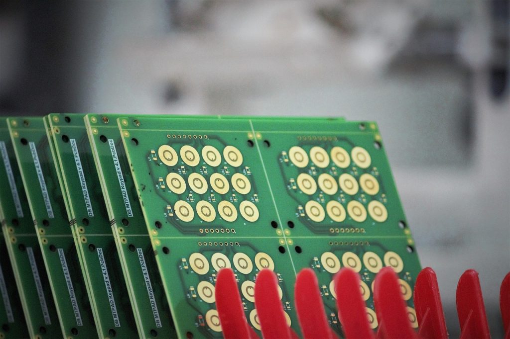
Quality Control and Inspection:

AI technology enhances quality control and inspection processes in electronic manufacturing. Visual inspection, a critical aspect of quality control, benefits from AI-driven machine vision systems. These systems employ deep learning algorithms to analyze images and detect defects, such as soldering errors, component misalignment, or physical damage. By automating the inspection process, AI technology improves accuracy, reduces human error, and increases throughput, ultimately ensuring higher product quality.

AI-powered machine vision systems can quickly and accurately identify defects that may be difficult for human inspectors to detect. This technology not only improves the efficiency of quality control but also reduces the likelihood of defective products reaching the market, thereby enhancing customer satisfaction and brand reputation.

Supply Chain Optimization:

AI technology offers immense value in optimizing the electronic manufacturing supply chain. By analyzing historical data, market trends, and demand patterns, AI algorithms can accurately forecast material requirements, manage inventory levels, and optimize procurement processes. This helps to minimize supply chain disruptions, reduce excess inventory, lower costs, and enhance overall efficiency.

AI algorithms can analyze vast amounts of data to identify patterns and correlations, enabling more accurate demand forecasting. By leveraging this information, manufacturers can optimize their production schedules, avoid stockouts, and reduce inventory carrying costs. Additionally, AI-powered algorithms can continuously monitor market trends and supplier performance, allowing manufacturers to make informed decisions regarding sourcing strategies and supplier selection.
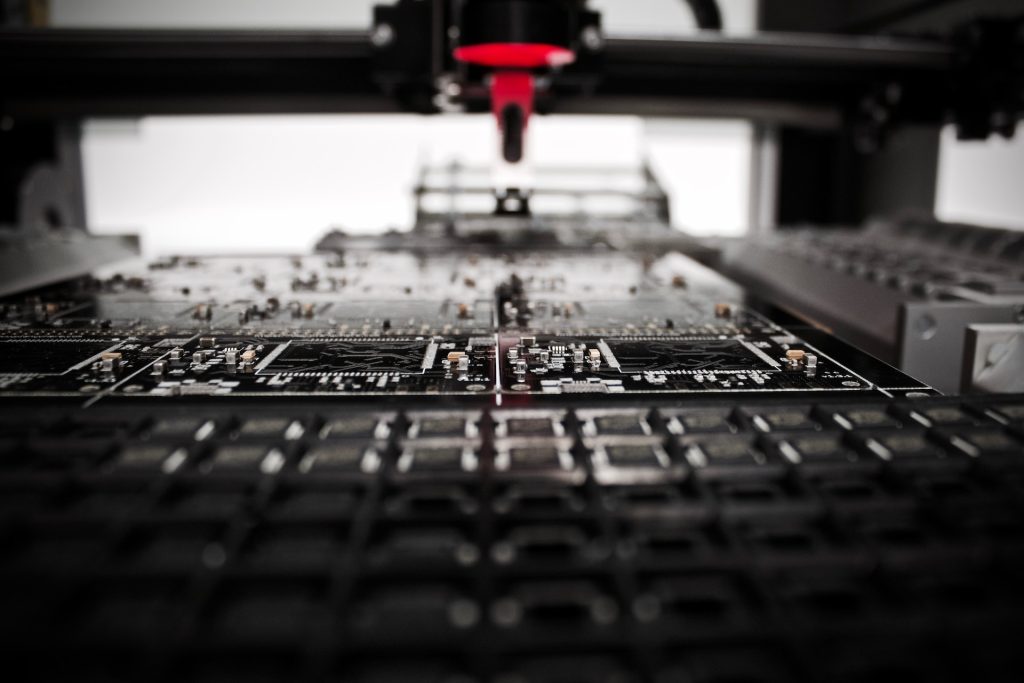
Process Automation:

AI technology enables process automation in electronic manufacturing, improving productivity and reducing manual labor. Robotic process automation (RPA) powered by AI algorithms can streamline repetitive and time-consuming tasks, such as data entry, documentation, and inventory management. This automation allows human workers to focus on higher-value tasks, leading to increased productivity, reduced errors, and improved overall workflow efficiency.

RPA can automate various tasks across the manufacturing process, such as generating production reports, updating inventory databases, or performing quality control checks.

Revolutionizing Electronic Design and Manufacturing: The Power of AI Technology Read More »

Exploring the Factors Affecting SMT Soldering Quality and Effective Solutions

Introduction

Surface Mount Technology (SMT) soldering plays a crucial role in modern electronics manufacturing, enabling the assembly of compact and efficient electronic devices. However, achieving high-quality solder joints can be challenging due to various factors that can impact the soldering process. In this article, we will explore some key factors that affect SMT soldering quality and discuss potential solutions to address them effectively.

Solder Paste Quality:

Solder paste composition: Ensure that the solder paste is formulated to meet the specific requirements of the components and the soldering process. Consider factors such as lead-free vs. leaded solder, flux type, and activity level.

Viscosity: Monitor and control the viscosity of the solder paste to ensure consistent and uniform deposition. Use viscosity measurement tools and adjust the paste or the printing process parameters accordingly.

Particle size distribution: Solder paste with a well-controlled particle size distribution provides better stencil release and improves solder paste printing quality. Regularly check the particle size distribution using laser diffraction or similar methods.

Soldering Temperature Profile:

Preheat: Ensure that the preheating phase brings the PCB and components to the desired temperature gradually, avoiding thermal shock and potential component damage.

Soak: Maintain a stable temperature during the soak phase to allow the flux to activate fully and promote proper wetting.

Reflow: Optimize the reflow profile by adjusting the ramp rate, peak temperature, and cooling rate to achieve the right balance between solder joint formation and minimizing thermal stress on the components.

Component Placement Accuracy:

Vision systems: Utilize advanced pick-and-place machines equipped with vision systems to align and orient components accurately. These systems can detect variations in component position, rotation, or polarity, reducing the likelihood of misalignment.

Calibration and maintenance: Regularly calibrate the placement machines to ensure precision and accuracy. Maintain and clean the nozzles, feeders, and placement heads to prevent any debris or misalignment issues.

Automated Optical Inspection (AOI): Implement AOI systems to detect and flag any component placement errors. This allows for immediate corrective actions, reducing the chances of soldering defects.

PCB Design Considerations:

Pad design: Optimize the pad geometry, including pad size, shape, and solder mask relief, to ensure sufficient solder wetting and proper solder joint formation.

Stencil design: Collaborate with stencil manufacturers to design stencils that provide consistent and accurate solder paste deposition, taking into account the component footprint and recommended solder paste volume.

Solder mask clearance: Maintain appropriate solder mask clearance around pads to avoid solder bridging and ensure proper solder joint formation.

Operator Training and Skills:

Comprehensive training programs: Develop training programs that cover the fundamentals of soldering, equipment operation, process parameters, and quality standards. Provide hands-on training to enhance the operators’ skills in component handling, solder paste application, and reflow techniques.

Continuous improvement: Encourage operators to stay updated with the latest industry trends and advancements through workshops, seminars, and certifications. Foster a culture of continuous learning and improvement within the organization.

Conclusion

Attaining high-quality soldering in SMT assembly is a multi-faceted process that involves addressing various factors that can impact the final results. By focusing on solder paste quality, optimizing the soldering temperature profile, ensuring accurate component placement, considering PCB design factors, and investing in operator training, manufacturers can significantly enhance their SMT soldering quality. Implementing these solutions will lead to improved reliability, reduced rework, and enhanced overall product performance in the ever-evolving world of electronics manufacturing.

Exploring the Factors Affecting SMT Soldering Quality and Effective Solutions Read More »

Unveiling the Effects of High Temperature and Humidity on PCB Performance

Introduction

Printed circuit boards (PCBs) are integral components in electronic devices, serving as the foundation for interconnecting and powering various electronic components. As electronic devices continue to advance, it becomes crucial to understand the environmental factors that can affect the performance and reliability of PCBs. In this article, we will explore the impact of high temperature and humidity on PCBs, shedding light on potential challenges and necessary precautions.

The Effects of High Temperature

  1. Thermal Stress: High temperatures can subject PCBs to thermal stress, which may lead to component failure or solder joint degradation. Excessive heat can cause expansion and contraction of the board and its components, potentially resulting in mechanical and electrical failures.
  2. Material Integrity: Elevated temperatures can adversely affect the material integrity of PCBs. The substrate material, typically made of fiberglass-reinforced epoxy, may experience thermal degradation, compromising the structural strength of the board.
  3. Signal Integrity: High temperatures can impact the electrical properties of the PCB, leading to signal integrity issues. Heat-induced expansion and contraction can alter the impedance characteristics of transmission lines, causing signal distortions or reflections.
  4. Component Performance: Electronic components on the PCB, such as integrated circuits (ICs), capacitors, and resistors, often have specified operating temperature ranges. Operating beyond these temperature limits can affect their performance, reliability, and even lifespan.

The Effects of High Humidity

  1. Corrosion: High humidity levels can create a conducive environment for the formation of moisture on the PCB surface. Moisture, in the presence of oxygen, can lead to corrosion of the conductive traces, solder joints, and component leads, compromising the electrical connectivity.
  2. Conductive Contamination: Humidity can contribute to the accumulation of conductive contaminants, such as dust, salts, or other pollutants, on the PCB surface. These contaminants can cause short circuits or interfere with signal transmission, leading to malfunction or reduced performance.
  3. Insulation Breakdown: Excessive humidity can deteriorate the insulation properties of PCB materials, such as solder mask or conformal coating. This breakdown may result in leakage currents, reduced insulation resistance, or even insulation failure.

Precautions and Mitigation Strategies

To mitigate the adverse effects of high temperature and humidity on PCBs, several precautions can be taken:

  1. Temperature Control: Ensure that electronic devices and PCBs operate within the recommended temperature range. Implement proper cooling mechanisms such as heat sinks, fans, or thermal management techniques to dissipate excess heat.
  2. Humidity Control: Use environmental controls such as dehumidifiers or humidity-controlled storage to maintain optimal humidity levels during storage, transportation, and operation of PCBs.
  3. Conformal Coating: Apply a conformal coating on the PCB surface to protect it from moisture, contaminants, and corrosion. This coating acts as a barrier, enhancing the PCB’s resistance to humidity-related issues.
  4. Enclosure Design: Employ effective enclosure design practices to prevent moisture ingress, ensuring that the PCB remains protected from high humidity environments.

Conclusion

High temperature and humidity can significantly impact the performance and reliability of PCBs. Thermal stress, material integrity concerns, signal integrity issues, corrosion, and conductive contamination are among the potential challenges. By implementing appropriate precautions such as temperature control, humidity control, conformal coating, and effective enclosure design, the detrimental effects of high temperature and humidity on PCBs can be mitigated. Understanding and addressing these environmental factors will contribute to the longevity and optimal functioning of electronic devices relying on printed circuit boards.

Unveiling the Effects of High Temperature and Humidity on PCB Performance Read More »

An Introduction to Printed Circuit Boards, What You Should Know

Introduction

In the realm of rapidly evolving technology, printed circuit boards (PCBs) serve as the backbone of electronic devices, powering and connecting them seamlessly. From smartphones to computers, PCBs play a crucial role in modern electronics. In this article, we will delve into the world of printed circuit boards, exploring their significance, construction, and various types.

What is a Printed Circuit Board?

A printed circuit board, or PCB, is a flat board made of non-conductive material that provides mechanical support and electrical connections for electronic components. It acts as a platform for assembling and interconnecting various electronic components using conductive pathways, or traces, etched onto its surface.

Construction of a PCB

PCBs are typically constructed in layers, consisting of a substrate layer, conductive layers, and a solder mask layer. The substrate layer is usually made of fiberglass-reinforced epoxy, while conductive layers, usually made of copper, are etched to form the desired circuitry. The solder mask layer provides insulation and protection to the copper traces, preventing accidental short circuits.

The PCB Design Process

The design process of a printed circuit board involves several crucial steps. It starts with schematic design, where the circuit is laid out using specialized software. The next step is the PCB layout, where components are positioned, and traces are routed to ensure proper connectivity. Once the layout is finalized, the PCB design is sent for fabrication, where the physical board is manufactured based on the design specifications.

Types of PCBs

PCBs come in various types, each serving different purposes:

  1. Single-sided PCB: Components and traces are present on one side of the board.
  2. Double-sided PCB: Components and traces are present on both sides of the board.
  3. Multilayer PCB: It consists of multiple layers of conductive material, allowing for complex circuitry and compact designs.
  4. Flexible PCB: It is made of flexible plastic material, enabling it to be bent or twisted to fit unconventional form factors.
  5. Rigid-Flex PCB: It combines rigid and flexible PCBs, offering both structural rigidity and flexibility.

Advantages of PCBs

Printed circuit boards offer numerous advantages over other wiring methods:

  1. Compactness: PCBs allow for compact and space-efficient designs.
  2. Reliability: They offer stable connections and reduced risk of loose connections or short circuits.
  3. Easy Repairs and Modifications: PCBs facilitate easier troubleshooting, repairs, and modifications compared to point-to-point wiring.
  4. Cost-Effectiveness: Once the initial setup cost is covered, PCBs can be mass-produced at a relatively low cost.
  5. Signal Integrity: PCBs are designed to minimize signal loss and interference, ensuring better overall performance.

Conclusion

Printed circuit boards form the foundation of modern electronics, providing the necessary connectivity and support for electronic components. Their construction, design process, and various types highlight their versatility and importance. As technology continues to advance, PCBs will undoubtedly evolve to meet the ever-increasing demands of the electronics industry.

Next time you hold a smartphone or power up a computer, remember the intricate world of printed circuit boards working silently behind the scenes, enabling our digital lives.

An Introduction to Printed Circuit Boards, What You Should Know Read More »

Expert Tips for PCB Assembly

PCB Assembly

Printed circuit boards (PCBs) are essential components of modern electronics, and the process of assembling PCBs is a critical step in the manufacturing process. PCB assembly involves several stages, including preparation, component placement, soldering, and inspection. In this blog, we will explore the different stages of PCB assembly and provide tips and best practices for each step.

Step 1: Preparation

The first step in PCB assembly is to prepare the PCB and components for assembly. This involves inspecting the PCB for any defects, such as scratches or damage to the solder mask. The components should also be checked for any defects or damage. Once the PCB and components are inspected, they can be prepared for assembly by cleaning and organizing them.

Step 2: Component Placement

The next step is to place the components on the PCB. This can be done by hand or with automated equipment, depending on the complexity of the PCB and the number of components. It’s important to place the components accurately and securely to ensure that they are in the correct position for soldering.

Step 3: Soldering

Soldering is the process of attaching the components to the PCB using solder. There are two main methods of soldering: through-hole and surface mount. Through-hole soldering involves inserting components into pre-drilled holes in the PCB and soldering them in place. Surface mount soldering involves attaching components to the surface of the PCB using solder paste and a reflow oven. Both methods require a high degree of precision and accuracy to ensure that the components are securely attached, and the solder joints are of high quality.

Step 4: Inspection

Inspection is a critical part of PCB assembly, and it involves checking the quality of the solder joints and the overall integrity of the PCB. This can be done using visual inspection or automated inspection equipment. Any defects or issues should be addressed and corrected before moving on to the next step.

Step 5: Testing

Once the PCB is assembled, it should be tested to ensure that it is functioning correctly. This involves electrical testing to check for shorts and opens and other tests to ensure that the PCB is functioning as intended. Testing can be done manually or using automated equipment.

PCB assembly is a complex process that requires specialized skills and equipment. It involves several stages, including preparation, component placement, soldering, inspection, and testing. By following best practices and using high-quality materials and equipment, it’s possible to create high-quality PCB assemblies that meet the required specifications and standards. Whether you’re a hobbyist or a professional, understanding the PCB assembly process is essential for working with electronics and creating innovative new products.

Expert Tips for PCB Assembly Read More »

Product Enquiry

Scroll to Top