
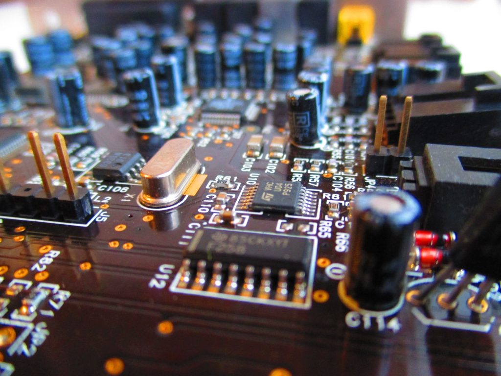
Printed circuit boards (PCBs) are essential components of modern electronics, and they are used in everything from smartphones to medical devices. PCB fabrication is the process of manufacturing these boards, and it involves several steps, including design, material selection, and manufacturing. In this blog, we will explore the different stages of PCB fabrication and provide tips and best practices for each step.
Step 1: PCB Design
The first step in PCB fabrication is to design the board. This involves creating a schematic diagram and a layout using specialized software. It’s important to consider factors such as the size of the board, the number of layers, and the placement of components. Once the design is complete, it can be exported as a Gerber file, which is used in the manufacturing process.
Step 2: Material Selection
The next step is to select the materials for the PCB. The most common materials used in PCB fabrication are copper-clad laminate and solder mask. Copper-clad laminate is the base material for PCB, and it comes in different thicknesses and substrate materials. Solder mask is used to protect the PCB from environmental factors such as dust and moisture. Other materials used in PCB fabrication include ink, plating chemicals, and adhesives.
Step 3: Manufacturing
The manufacturing process for PCBs involves several stages, including drilling, plating, and etching. First, the PCB is drilled to create holes for components and traces. Then, a plating process is used to coat the holes with copper. Next, a layer of solder mask is applied to protect the PCB. Finally, the PCB is etched to remove any unwanted copper and create the desired traces and connections.
Step 4: Quality Control
Quality control is an essential part of PCB fabrication. It involves testing the PCB to ensure that it meets the required specifications and standards. This includes visual inspection for defects, electrical testing to check for shorts and opens, and other tests to ensure that the PCB is functioning correctly.
Step 5: Assembly
Once the PCB is manufactured and tested, it can be assembled with components to create a functional electronic device. This process involves placing the components on the PCB and soldering them in place. This can be done by hand or with automated equipment.
PCB fabrication is a complex process that requires specialized skills and equipment. It involves several stages, including design, material selection, manufacturing, quality control, and assembly. By following best practices and using high-quality materials and equipment, it’s possible to create high-quality PCBs that meet the required specifications and standards. Whether you’re a hobbyist or a professional, understanding the PCB fabrication process is essential for working with electronics and creating innovative new products.