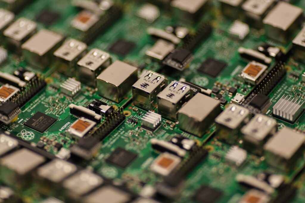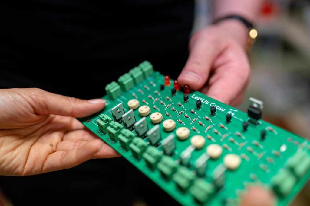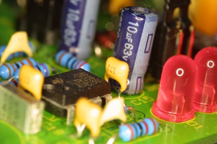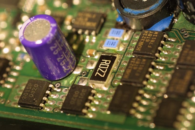
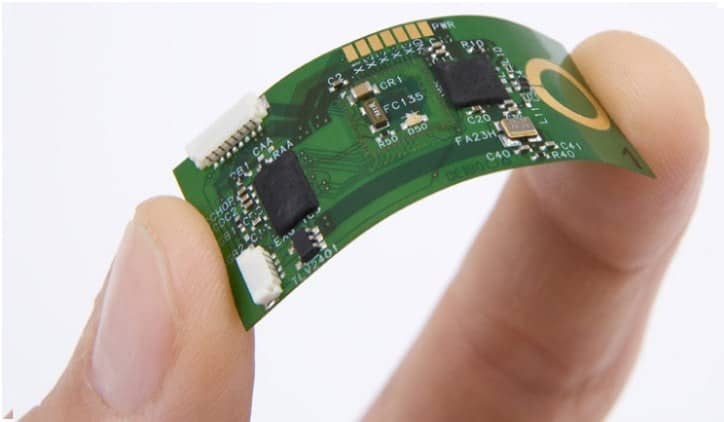
What is a Flexible Printed Circuit Board (PCB)?
OPTIMIZATION OF POLYMERIC STRUCTURE OF ORGANIC PRINTED CIRCUIT BOARDS (PCB)
POLYMERIC STRUCTURE OF MULTILAYER FLEXIBLE PRINTED CIRCUIT BOARDS – ”Sulaiman Khalifeh, in Polymers in Organic Electronics, 2020“
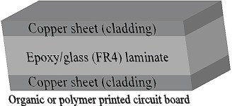
The polymeric printed circuit boards (also called “organic printed circuit boards”) PCB are the simplest self-assembled structures of interconnected microelectronic/Nano-electronic components on a thin film substrate formed from polymer-based composites such as epoxy. As illustrated in Figure 5.1, such structure has several advantages, including very low cost, good electromechanical properties, easy to manufacture in any shape, and applicable for multilayer configurations. These printed circuit boards can be electrically connected to organic/polymeric circuits by either “through-hole technology” THT (older process) or “surface mount technology” SMT (newer process). A more recent solution includes “integrated circuits” IC (also called “microchip”) by which the polymeric printed circuit boards can be built with more circuits and components that are electro-chemically grown in place on the surface of a very small chip. The other method is called a “hybrid circuit” that contains some components, which can be grown onto the surface of the substrate without the need to be mounted on the surface and soldered.
Three-dimensional polymeric printed circuit boards 3D-PCPs are the most developed solutions, where both single-sided or multilayered polymeric printed circuit boards can be fabricated in the form of 3D-prototypes depending on the “miniature technologies” such as “molded interconnect device” MID. With molded interconnect device technology, the copper traces act as an electrical circuit on the polymeric substrate that can be fabricated by “two-component injection molding,” “hot stamping, photolithography,” “in-mold circuit film,” or “laser direct structuring” LDS which can be considered as the most flexible technology. Such a process can be called “three-dimensional molding of interconnected devices” 3D-MID, while the resultant product can be called “three-dimensional printed circuit board” 3D-PCB as illustrated in Figure 5.2. The direct laser structuring can be achieved immediately after applying single-component injection molding of the carrier. Examples of polymers used for fabricating the polymeric substrates by injection molding process include: liquid crystal polymers LCP, poly(butylene terephthalate) PBT, Trogamid® (amorphous polyamide) (known as: PA 6-3-T), and poly(ethylene terephthalate)/poly(butylene terephthalate) blend PET/PBT.
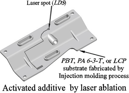
[Data from Laser Micronics GmbH, 3-Dimensional Circuitry, Laser Direct Structuring Technology (LPKF-LDSTM) for Molded Interconnect Devices, 2012.]Copyright © 2012.
The concept of “optoelectronic printed circuit boards” has been developed to satisfy the increasing demand for high data rates along with progressive miniaturization of devices and components. Optoelectronic printed circuit board represents the integration of optics in a polymeric printed circuit board that is the need to utilize optical fibers, the generation of waveguides by UV lithography, embossing, or direct laser writing. An example of commercial polymers used for structuring optoelectronic printed circuit boards is Ormocer®, which is a type of inorganic/organic hybrid polymer.
POLYMERS FOR CONVENTIONAL PRINTED CIRCUIT BOARDS
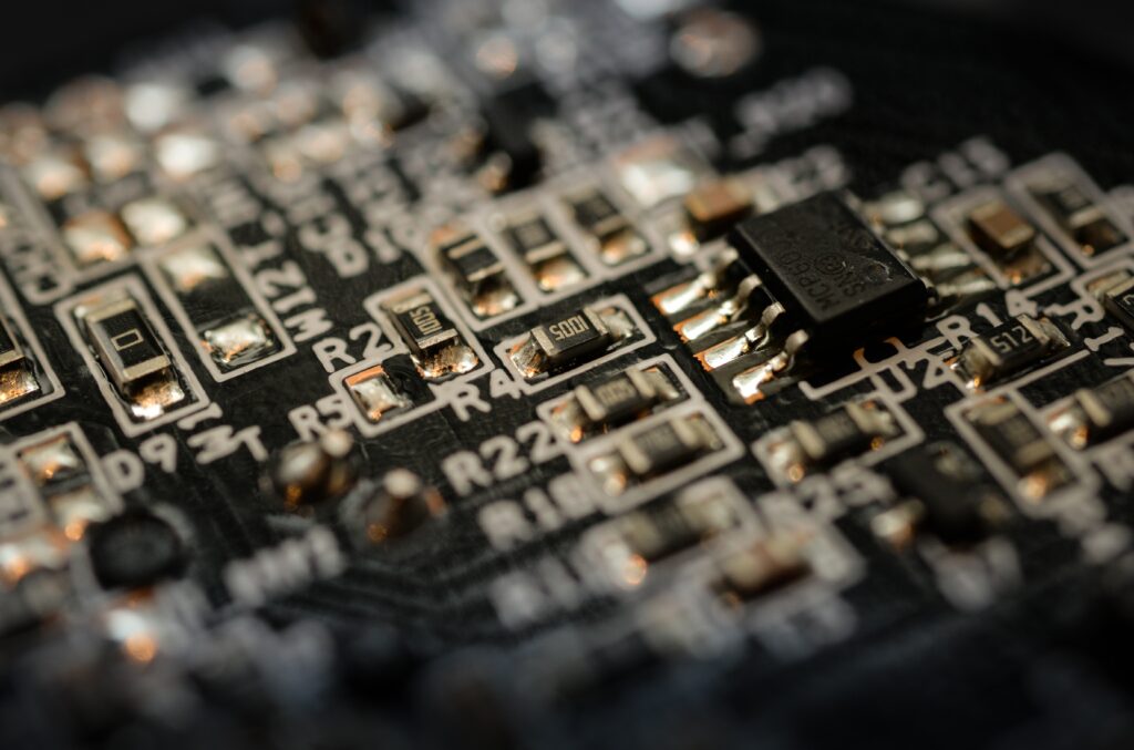
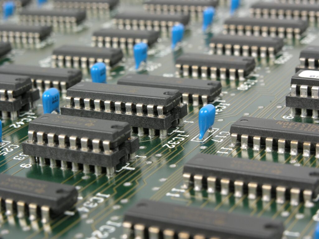
The main function of printed wiring is to support circuit components and interconnect these components electrically. Several types of flexible and rigid printed wiring have been used, including traditionally printed circuit boards (single-sided, double-sided, and multilayered), ultra-multilayered printed circuit boards, and three-dimensional printed circuit boards. These types are based on variable dielectric materials (polymers and composites, conductors types, number of conductor planes, rigidity, flexibility, etc.) Rigid printed circuit boards of substrates formed from thermosetting polymers, such as epoxy composites, and flexible printed circuit boards of substrates formed from thermoplastic polymers (such as polyethylene terephthalate PET) are the main two types. Thermosetting composites can be used in the form of filled or glass fiber reinforced epoxy resin EP-GFR, while paper reinforced phenolic (phenol-formaldehyde PF) resin with a bonded copper foil or silicone Q substrates is used for fabricating very small chips (microchips) and stretchable circuits.
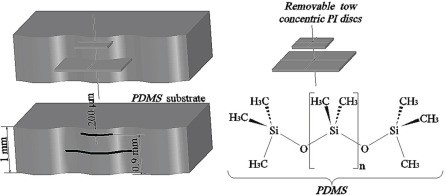
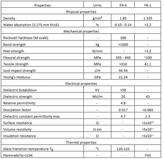
The first optimized type of glass fiber reinforced epoxy resin used for structuring conventional printed circuit boards is available in the form of epoxy glass, fire-retardant grade-4 (abbreviated as FR-4). It has very high thermal stability, good mechanical and electrical properties, flame retardance, excellent bonding to copper foil, electroless copper, and glass fibers. It is approved by National Electrical Manufacturers Association NEMA for synthetic resin bonded papers. FR-4 is a polymeric composite material made of woven glass impregnated with plasticized epoxy resin. The second optimized resin is phenolic glass, fire-retardant grade-2 (abbreviated as FR-2), which is a composite material made of paper impregnated with plasticized phenol-formaldehyde resin for the same application. The third optimized type is silicone, which has been used as a flexible substrate for fabricating hybrid stretchable circuits (Figure 5.3). It consists of a millimeter thick polydimethylsiloxane PDMS (IUPAC name: polydimethylsiloxane) having the formula ((C2H6OSi)n) within which two concentric discs of polyimide PI foil (50 µm thick) are embedded. It is a derivative of polyorganosiloxane used as packaging polymer for electronic devices, as well. Polydimethylsiloxane is the first optimized derivative of silicone family used for structuring polymeric double-disk stretchable substrate due to its high strain property. Note: polymeric materials used for fabricating printed circuit board substrates are made of differential dielectrics. This means that they can be selected to provide different insulating values depending on the requirements of the circuit. For this reason, the two types of substrate that can be selected for traditional printed circuit boards are dielectric printed circuit boards and prepreg printed circuit boards.
DIELECTRIC SUBSTRATE-BASED POLYMERIC PRINTED CIRCUIT BOARDS
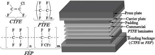
The dielectric materials (including most polymers) are insulators (non-conducting electricity) resisting the flow of an electrical current. Dielectric polymer represents the optimized class of dielectric materials used for dielectric substrate-based polymeric printed circuit boards, including polytetrafluoroethylene PTFE, epoxy glass, fire-retardant grade-4 (FR-4), epoxy glass, fire-retardant grade-1 (FR-1), composites of epoxy with cotton paper (CEM-1), and composed of nonwoven glass core combined with epoxy resins (CEM-3). The laminates of thermoplastic polymer polytetrafluoroethylene represent the first member of dielectric polymers used for antennas and base stations because of their high melt viscosity. The laminates are fabricated under the lamination pressure of 3.1-3.27 MPa.
An example of commercial polytetrafluoroethylene grade used as a polymer for structuring the substrate of double-sided printed circuits is Teflon®. Figure 5.4 is an example of multilayer laminate containing polytetrafluoroethylene used for printed circuit boards. Polytetrafluoroethylene is bonded with chloro-trifluoroethylene CTFE (IUPAC name: 1-chloro-1,2,2-trifluoroethene) having formula C2ClF3 or fluorinated ethylene-propylene copolymer FEP produced by free-radical polymerization of mixture of hexafluoropropylene and tetrafluoroethylene.
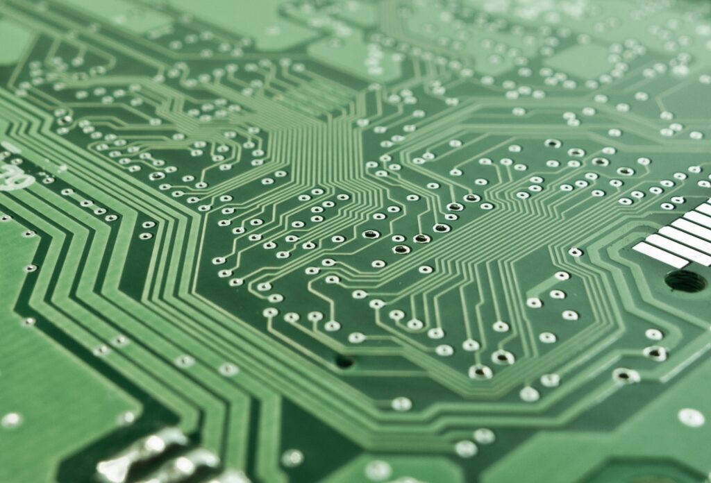
Epoxy glass, fire-retardant grade-4 FR-4 is the second optimized grade for structuring dielectric substrate-based polymeric printed circuit boards due to its very good mechanical and electrical properties, ability to resist flame, and excellent bonding to copper foil, electroless copper, and glass fibers. Epoxy is available as “difunctional-epoxy” DfEP blend formed by reacting epichlorohydrin and bisphenol-A with flame-retardant additive, “tetrafunctional epoxy” TfEP blend, and “multifunctional epoxy” MfEP blend, listed in Table 5.1. Importance of epoxy polymer is in acting as self-extinguishing binder (self-extinguishing term is used to describe the ability of a material/polymer to cease burning upon removal of the source of flame). Epoxy glass, fire-retardant grade-4 available in the form of laminate is resistant to high temperature and water absorption\, has good electrical insulation, and good machinability. To optimize both physical and electrical properties of the laminate, its glass fibers should be made perpendicular to one another. Some of these properties are listed in Table 5.2. An example of epoxy glass, fire-retardant grade-4 (FR-4) two-layer structure is illustrated in Figure 5.5. Such structure consists of a woven glass fiber mesh soaked in the organic polymer (epoxy as resin matrix) with copper layers laminated (sometimes filled with specific materials).
| Properties | Units (condition) | Difunctional epoxy DfEP blend | Tetrafunctional epoxy TfEP blend | Multifunctional epoxy MfEP blend |
| Glass Transition Temperature | °C | 130 | 130 – 140 | 160 – 190 |
| Dielectric constant | at 1MHz | 4.5 | 4.6 | 4.4 |
| Dissipation factor | at 1 MHz | 0.025 | 0.025 | 0.025 |
| Moisture absorption | % | 0.70 | 0.06 – 0.013 | 0.60 – 0.013 |
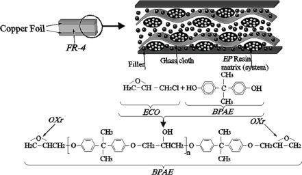
According to Figure 5.5, and Table 5.1, the polymeric matrix of epoxy glass, fire-retardant grade-4 FR-4 laminates consists of bi-, tetra- or multi-functional epoxy groups. Note: epoxy EP is chemically derived from the reaction of bisphenol-A epoxy BPAE with epichlorohydrin ECO which creates diglycidyl ether of bisphenol A (DGEBA) (also referred to as oxirane OXr). OXr (DGEBA) reacts in subsequent resin polymerization, curing the polymeric matrix. Higher crosslinking in the cured system can be achieved by the use of epoxy monomers with more than two epoxy functional groups per molecule.
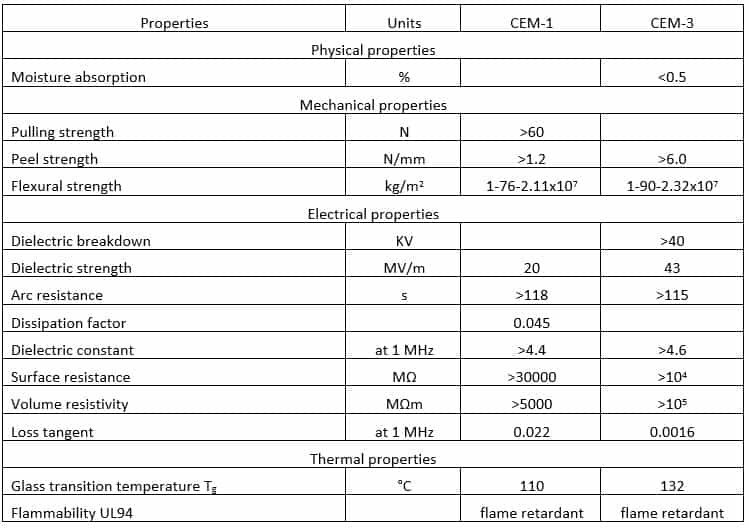
Epoxy glass, fire-retardant grade-1 FR-1 is the second optimized epoxy glass, fire-retardant grade used in dielectric substrate-based polymeric printed circuit boards. It is a thermoset polymeric composite formed from the paper base with plasticized epoxy resin. Properties of this composite were listed in Table 5.2. Composite of epoxy with cotton paper (abbreviated as CEM) represents the third optimized class of polymeric composites used for structuring dielectric substrate-based polymeric printed circuit boards. These composites are commercially available in the form of five numbered grades, including CEM-1, CEM-2, CEM-3, CEM-4, and CEM-5. Where numbers from 1 to 5 are related to the type of the base. For example, number 1 means cotton (or cellulose) paper and epoxy.
CEM-1 is a polymeric composite consisting of woven glass fabric surfaces and paper core combined with epoxy resin. It is easy to punch, and has excellent mechanical and electrical properties, and higher flexural strength than paper-based grades. It is used in radio receivers, smoke detectors, and single-sided printed circuit boards. Its properties are listed in Table 5.3. CEM-3 is a composite of nonwoven glass core combined with epoxy resin. Similarly to CEM-1, it consists of epoxy resin with woven glass cloth surfaces, but its core is nonwoven matte fiberglass. The nonwoven mate fiberglass optimizes through-hole plating. It has better fine-line capability than FR-4. It has a very smooth surface and milky white color. It can be used as an alternative to FR-4, known as a flame retardant epoxy copper-clad plate glass material.
What is a Flexible Printed Circuit Board (PCB)? Read More »